
PCB Designing with Altium Designer – Hardware Development
Welcome to a series of Articles on Hardware Development. In this series, we are gonna walk through the PCB Designing & Manufacturing of Li-Ion battery charging Hub. I’m gonna design this PCB with Altium Designer 20 and then we will get this PCB manufactured by PCBWay.com
Table of Contents:
PCBWay :
We all know that PCBWay.com is an online PCB ordering platform where we get the PCBs delivered at our home with very simple steps. Currently, PCBway.com started PCBWay BIG SALE due to Christmas, there are so many exciting offers, Also, they are offering 10 pcs of 2 layered PCBs at just $5, Get your PCBs ready by PCBWay.com now. PCBWay.com is the one-stop solution for PCB Prototyping, Manufacturing, and PCB Assembly. Along with PCB prototype and SMD-Stencils PCBWay is also providing PCB Assembly within 3-4 day production time. get your PCBs ready at PCBay.com
Altium Designer:
Altium Designer is the standard for PCB design.
This is because, it’s an all in one feature-rich design environment with a modern, powerful, and unique approach to design.
whether you’re designing smaller or large simpler or complex, Altium designer has you covered with support for high-speed HDI and rigid-flex there’s nothing it can’t a candle.
one of the main technologies behind all these capabilities is the industry-leading interactive routing engine which is able to push self objects length too but they built in the electromagnetic fields over and out at any angle.
schematic captured is agile and intuitive enabling uses to design flat in hierarchical projects with ease.
into dynamic data model together with a continual compilation the last for instant availability of a netlist and project structure changes as well as rapid access and editing of the components properties models and parameters
Altium designer for manages data in a convenient and transparent manner with status in life cycle controlled by having all data in one place you just came effortlessly create complete documentation packages for manufacturing and assembly in seconds
a beautiful and modern an intelligent unified user interface brings out the full power of your tools in a platform that easy to use and simple to understand this means lower learning curve allows you to be proficient in almost no time at all. and with the world’s largest international community of electronics design professionals, you’re never alone…
That’s why I choose Altium.
Not only me, Altium is widely used by all the multinational companies in the field of electronics like Texas Instruments, ST microsystems, Seimens, Seagate, Philips, Microsoft, Lenovo, HP, and some other companies like Audi, Boeing, Broadcom, and Even NASA is also using these Altium Products for their design.
So, Let’s see how we can Design our PCB with Altium Designer. I assume you have already downloaded and installed Altium Designer and completed the necessary onboarding steps of Altium Designer Software.
If you didn’t do that, You can download Altium Designer 20 from here and follow the instructions to complete the setup.
So, without wasting time let’s get started.
Schematic Design with Altium Designer:
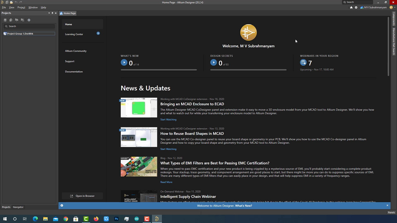
Launch the Altium Software from the Windows menu. It will take less than 2 minutes to load the software based on your system performance.
On the Altium Designer Home page, we can get the Latest Articles and Videos of the News and Updates of the Altium designer. We also have a Learning center, Altium Comunity, Support, and Documentation.
On the left side of the screen a project panel ill be there, Altium uses panels to provide access to information and tools. To access the list of possible panels in Altium designer left click on the panel’s button which is at the bottom right corner of the window. This opens up a menu with the various entries. the panels with checkmarks are currently open, and others are not open.
Coming to the main menu, We have options like File, View, Project, Window, and Help.
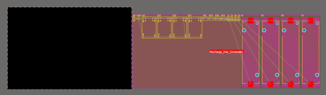
To create a blank project, click the file, new project. This enables a create project window to pop-up. while there are many options here we will start with the typical piece of the project with a default PCB. we can also give the custom name to the project, we will name the project “Recharge_Hub and create it”.
An Altium Project file will be added to the projects panel, In this project, we can add schematics by right-clicking on the project file name, and selecting “add new to project” then select a schematic. a new blank schematic file will be added to this project with a default name. We can also add a PCB file to the Project in the same way, then save them with the proper name.
Below is the Simple circuit to charge Lithium-ion batteries with TP4056, we have already covered this part in the previous article. If you miss it by chance, complete reading it, and then come back to here.
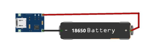
So, to place this Li-ion battery on PCB, We need a battery holder. I found this SMD battery holder which is perfect for 18650 batteries. Add this component to the schematic. There are 2 ways to import components to Schematic, 1. Components it has default components, and the 2. MFR part search, This is an online searching tool.
Adding a Battery Holder to the Schematic:
The manufacturer no is 1042p, we can search in both ways by using this mfr no. but In Altium components & in mfr parts search, the part 1042p is not available. thus we cannot add this to the project. So, the only way left is to install the Altium Library loader.
Visit the Altium library installation page, download the file. Extract it. Rename it as “.exe” and then Install it. Please note that whenever you are installing this software the Altium should be closed.
After installation of the tool, relaunch the Altium software. Now you can see Altium Library loader in the file menu and tolls menu as mentioned in the instruction guide. Now, launch that tool and search for the 1042P part. verify the part and click on add to design. That’s it, the Battery loader added to the schematic, and that can be found on the bottom left corner of the schematic diagram. place this component in the middle of the
Adding a TP4056 to the Schematic:
Now, the next task is to add the TP4056 module to the schematic, In components and Mfr part search Tp4056 is not available. it is also not available on the Altium Library loader. Altium can help us to solve it, that’s why Altium is the standard PCB designer.
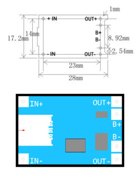
In Altium, there is a feature to design our schematic libraries and PCB libraries which are not available anywhere. To add PCB libraries to the project, go to the project and select “add new to project” and then select “PCB library” A blank PCB library file will be added to the project. rename with a proper name and save it. To design a PCB library, we should have the measurements of the desired component. Here are the blueprints of the TP4056 which has all the required measurements.
There will be a mark on the screen which is called the origin point of the PCB library file. If you move the cursor, you can see the values of x and y coordinates are changing according to the cursor movement. the values will be in mils format, the thousandth part of an inch is called as one mil. I have clearly explained the PCB library designing in the video tutorial, you can watch it for better understanding.
First place a pad at the origin point, then calculate the coordinates of the rest of the pads using x, y coordinates as a guide and place them in their respective place.
The calculated coordinates will be as follows.
| PAD | X | Y |
| IN+ | 0 | 0 |
| IN- | 0 | -550 |
| OUT+ | 905 | 0 |
| OUT- | 905 | -550 |
| B+ | 905 | -100 |
| B- | 905 | -450 |
Place all 6 pads at their respective coordinates, rename them with their proper names.
Draw a line on the top silk layer with an outer boundary with 60 mils distance. Also, annotate each pad on the top silk layer. After completing all these steps, save the file with the proper name. After all these steps the PCB Libray may look like this.
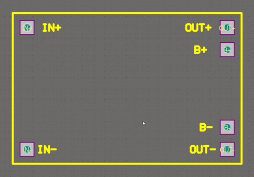
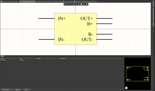
The next part is to create a schematic library for tp4056, Schnematic library is just a representation of pins, To add Schematic libraries to the project, go to the project and select “add new to project” and then select “schematic library” A blank schematic library file will be added to the project. rename it with a proper name and designator and save it. place a rectangle to represent the TP4056 module. Then place pins to connect with external circuitry, Make sure the name of the pin should be in the rectangle box, To avoid confusion, place the pins similar to the Actual TP4056. Then attach the PCB library file to the Schematic library. For that click on the properties panel, you can find the “Add” option at the bottom, click on that, and select foot print option. This enables a PCB model selection window to pop-up, select the recently created PCB footprint model, and click on okay. This will attach the PCB Footprint model to the schematic. Then save this library with the proper name. After all these steps the schematic library may look similar to this.
Now install this newly created library. for that go-to components, click on the hamburger menu, and select file-based library preferences, this enables the Available file-based library selection window to pop-up, select the newly created libraries, and click on the “add library” option, This will pop-up a file manager window to select the real files. Select both library files and click on open. Then close the Available file-based library selection window. Now, the Libraries are installed, and you can find them in the Components dropdown menu.
Now, go-to components dropdown menu, you can find the newly installed libraries here, select the schematic library, right-click on it and Select place option,
The Component will be attached to your cursor, you can take that wherever you want on the screen and place it by clicking on the left click. you can rotate the component by pressing the space bar.
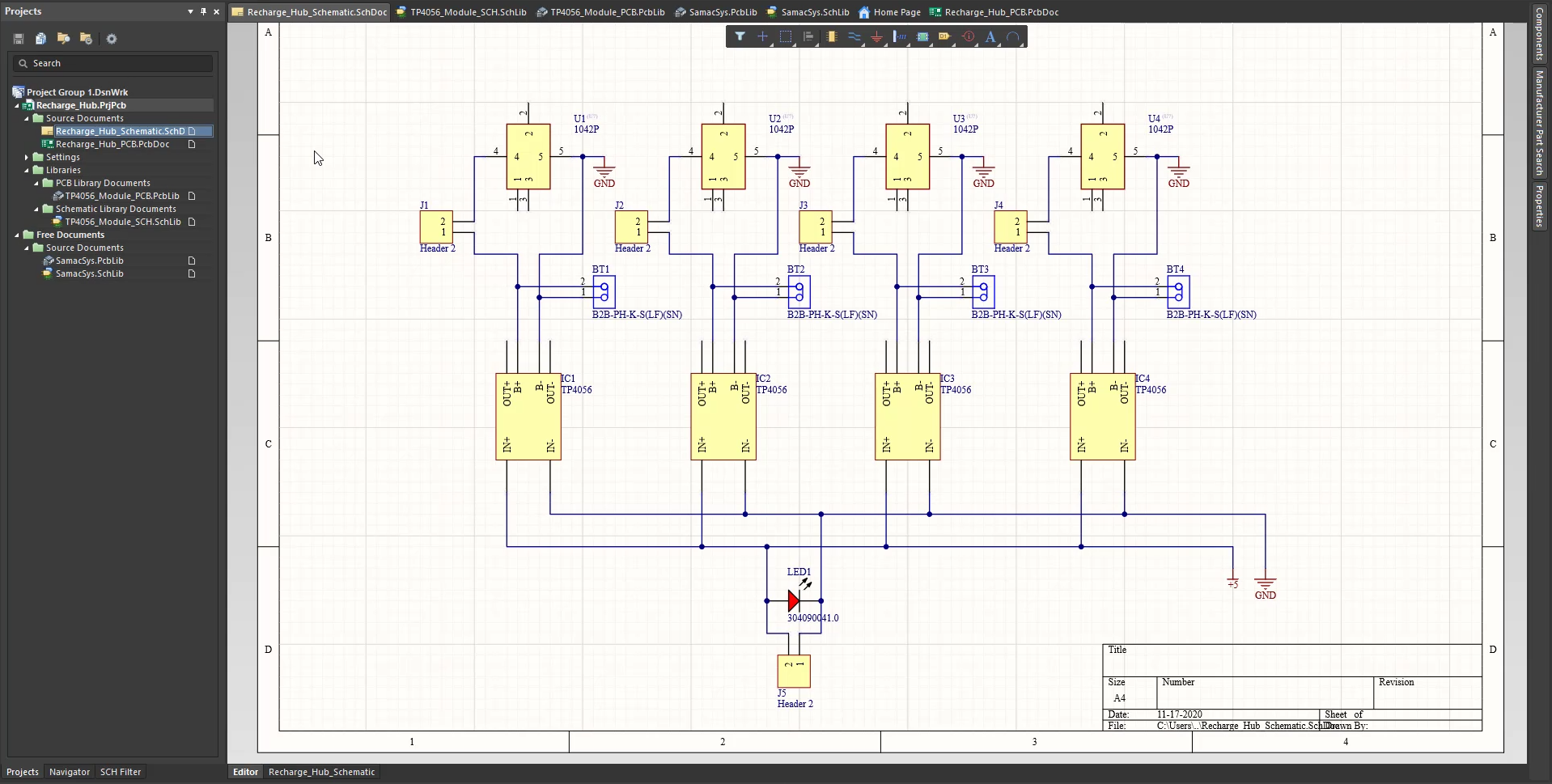
Now, the main components to charge a single 18650 battery are added to the schematic. add 2 more components to this circuit, one is a 2 pin male header, which is going to use as a switch. the second one is a battery connector to provision another lithium-ion flat battery. Go to the Components panel, select the miscellaneous connectors option and type header2, place the component. search the battery connector in the mfr search, type mfr no B2B-PH-K-S(LF)(SN), so place the component.
All required components are added to the sketch, arrange, and connect. The male header should be connected in series to act as a switch, the battery connector should be connected in parallel to the 18650 battery holder. this can charge only one battery, replicate the same circuit for the other 3 batteries, as we wanted to make a recharging hub to charge up to 4 batteries. Add Input Status LED and a male header for external input. short all input of the TP4056 and connect led and Input male header. then add a nets 5v and GND to the respective nets. Also, add a ground net to the battery negative terminals.
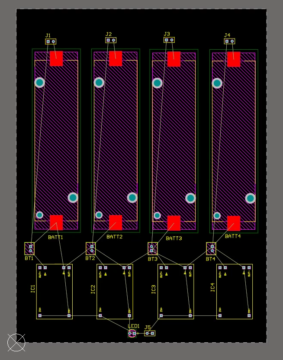
The final schematic will be something like this. Save all the files before jumping into the next step.
The next step is to add all these components to the PCB file, Arrange and Connect them according to the schematic, then generate the PCB manufacturing files.
PCB Design with Altium Designer:
I have clearly explained the PCB Routing in the Video tutorial, you checkout for better understanding.
Now we are ready to transfer the design to the PCB, To do that first go to the design pull-down menu and select Update PCB Recharge hub. This enables a window to pop-up which contains every detail of action we performed, the Affected object, and affected document and all. if the project was not compiled, the tool will compile it and create a unified data model of the design. the unified data model or UDM provides the linking between the schematic and the PCB.
First of all, we need to validate changes, and then we can execute the changes. To do that, click on the validate changes button, it will validate all changes we have performed and gives a status indication. a green tick means passed and a red tick means failed. Hopefully, we have passed all the validation changes. Now click on the execute changes, This will execute all the changes and update all passed changes to the PCB document, this will also show status indication whether it is executed or not. if there is no error all of the changes will be executed and components are updated to the PCB file. Then close the window.
After transfer, the PCB will look like this.
At this stage, we have a two-layer PCB with components showing their connectivity. as you can see the parts are placed off the PCB and are in a group called room. this room is auto-generated based on the schematic.
First of all, I prefer to set the origin of the board to the lower-left corner. To do this open the Edit pulldown menu and select origin and then select set, now with the mouse we can place the (0,0) coordinates for the port by selecting the bottom left corner of the PCB and then left mouse click as shown here. we will change the board size from the default dimensions. we will be changing the board size to 4.725 by 6.3 inches. To edit the board shape we need to enter into the board planning mode by hitting the number 1 key, with the PCB now green indicating we are in the edit mode, we can directly work on the PCB using the design pull-down menu. select the Edit board shape option to allow us to pick on the vertices of the board and move them. we could adjust the height and length of the board using the x and y coordinates as a guide the coordinates reflect the current mass position, we will set the board to the desired 4.725 by 6.3 inches size and then deselect, to switch back to 2d mode hit the number 2 key. Now the board size is edited, the next thing is to transfer all the components from the room to PCB.
While Placing components on the PCB, we need to make sure that, controlling components should be easily accessible and the wiring between the components should be minimized as little as possible.
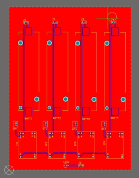
First of all, I am gonna place these 4 battery holders on the upper side, then the TP4056 modules on the lower side. Then input Male header and Input status led at below the TP4056 module, and battery connectors are going to place between the TP4056 modules and Battery holder. Finally, Male headers which are going to use as switches are placed on top of the PCB. Now All the components are placed on the PCB, we will continue moving parts and utilizing connection lines to fine-tune the placement of the PCB, I will use few lines to re-arrange the components to maintain the symmetry between components. this will allow us to make PCB look beautiful. here is the final placement of the design,
while this design does not require placing the component on the bottom side, all components are placed on the top layer only.
PCB Routing:
looking at the PCB, we see there are empty and through-hole devices. this provides us with top and bottom layers as routing choices. now let’s make a start on a layout by selecting the top layer and doing some manual routing, we will use the interactive routing for this. This can be selected from the active menu on the top. at this point, we can simply click on the pin we wish to start routing then move away and finish routing by making the connection with the other pin, since we are on the top layer the track will be in red. we can open the properties panel, by double-clicking on the routed track, You can see the properties of the track here. As you can see here the track width is 10 mils which are the default for signal tracks, but in our project, we are using it for charging the Batteries, So it is better to have a more track width to deliver more current, So I have decided to have a 1 mm track width. if we convert 1mm to mils, it is around 40 mills. So let’s enter the same thing here. THe 40mils track will be something like this.
If I wanted to have a 40 mils track width I should edit every track after routing which is a difficult task. So, we can configure the default width from the properties panel. here you can see that all the width preferences are set to 10mils, first, we need to change that. to do that, go to the pull-down menu Design and select rules. this will enable a PCB rules editor window to pop-up.
there are a bunch of categories of rules, select routing category and then select width option, because the track width has belonged to the routing category only. Here we can edit minimum width, preferred width, and maximum width.I want to keep the maximum width of 100 mils, the preferred width is 40 mils and the minimum width of 10 mils. Then click on apply, then click on okay.
Now go back to Properties and select preferred width 40 mils. that’s it, from now onwards every track we will route will have 40 mils width. let’s start routing by simply clicking on the pin we wish to start routing then move away and finish routing by making the connection with the other pin. then repeat the same thing with other Input pins too. Here I am not allowed to route the connection between these two pins, because there is a ground line. So, I will simply connect these two pins to the bottom payer. since we are on the bottom layer the track will be in blue. Then We will continue to route the rest of the 5v net tracks between the battery, Tp4056 module, and battery connector. So, Now all the Positive net tracks are routed.
The Ground net tracks are left unconnected. But we are not gonna connect them with general routing. we will use another technique. to provide these connections we use polygon planes. Go to the Active menu and select Place polygon plane, before we place the polygon, hit the tab key, so we can pause the polygon pour mode and edit the properties of the polygon. in the properties window, change the net from no net to GND from the drop-down list, and hit enter. now we can place the vertices of the polygon at the four corners of the PCB as shown here. Now we have placed a polygon on the bottom layer. let’s hide this layer and continue to place the polygon on the top layer. Repeat the same thing with the top layer too.
That’s it, the polygon layer is also poured on the top layer. as you can see any through-hole pin that has GND assigned to it, is automatically connected to the polygon. the SMT pins that also need connections to the GND are automatically connected to the polygon. So, the routing part is completed.
Now let’s enter into the branding part.
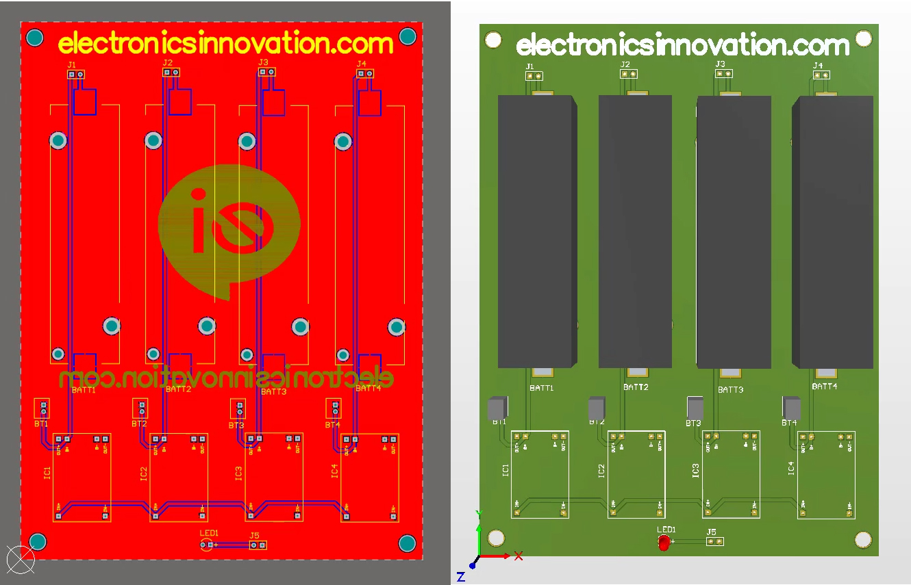
I want to place my website URL on the top silk layer. we will use the string option for this. Also placed the website URL and the logo of my youtube channel to the bottom silk layer. thus the branding part is also completed. The final PCB in a 2d model will look as shown in the below picture.
Altium provides a 3d model feature to see the PCB layout in 3D View as it can give us a real-life perspective of the placement and layout. To enable 3d mode just hit the number three key, This is how our PCB looks in 3d View. To rotate the view in 3d, hold the shift key to get the trackball to appear, and then use the right mouse button to rotate the 3d view. we can play with this feature, this gives us some sort of satisfaction with the work that we have done. I enjoy playing with this feature. To reset the 3d view click on the number 2 key.
So, that’s it, the PCB designing process is completed, let’s save all the files first.
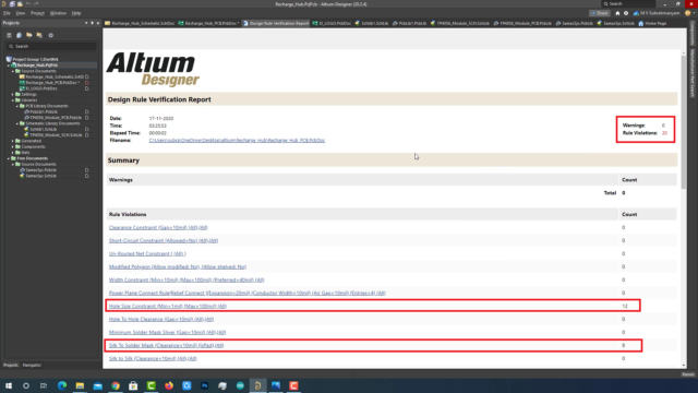
The only thing left is to generate the fabrication file. but before going to that process, we need to perform the DRC, which also stands for design rule checker. This will validate our design and checks whether our PCB obeying all the Design rules or not and also check for any other violations. this will help us to minimize future problems and solve them at the design stage only. So, let’s do that first.
To do that, go to the Tools pull-down menu, and select the Design Rule Check option, This will enable the design rule checker window to pop-up, click on the run design rule check option from the bottom right corner of the window. This will generate a Design Rule Verification report. Here it is showing a total of 20 violations which are 12 violations of Hole Size constraints, and 8 violations of silk to solder mask clearance. Let’s see what are these violations, Hole Size constraints, here it is showing the hole size is 135mils, but the rule is stating it should be less than 100 mils, but this is okay, because itis from the Battery footprint itself, So, we can waive it. Then silk to solder mask clearance is also from the footprint itself. So, we can waive it and move forward. Close the report. and save the project files.
At this point, we are now ready to generate the needed files for fabrication which include Gerber and NC drill files for PCB fabrication and pick-and-place files for PCB assembly. To generate the needed Gerber files use the File pulldown menu and select fabrication outputs and then select Gerber files, this opens up the Gerber setup window. Here we can review and change settings to suit our fabrication requirements Under the general tab, we will select 2:3 for the format, as we do not require very high precision. clicking on the layers tab, we need to select which layers to plot for the Gerber files. there are no layers selected by default, I often select used on from the plot layers pulldown menu at the bottom left corner of the window, this allows the tool to plot all the used layers in this PCB. under the drill drawing tab I usually select plot all used drill pairs for both sections, click OK to start the generation process After Gerber generation has done the CAMtastic viewer opens with the various layers plotted. we can see the file generated under the generated folder in the Project panel We have our Gerber files, so just close this file and do not save it
let’s generate the NC drill files using the file pulldown menu, fabrication files, and then selecting NC drill files. this opens up the NC drill setup window. we will keep the defaults but change the format 2:3 and click OK, Click OK again, After NC drill files generated, the CAMtastic NC drill drawing viewer opens, We can see the drills on this view. I normally close and do not save this view.we can see the file generated under the generated folder in the Project panel now we have the Gerber files and NC drill files generated
now we can generate the pick-and-place files using the file pulldown menu, and assembly output and selecting generate pick-and-place files this opens up the pick-and-place setup window, where we can configure the pick-and-place file for our particular vendor and output either CSV or text depending on what is needed clicking ok generates the files. we can see the just generated pick-and-place file under the generated folder in the Project panel.
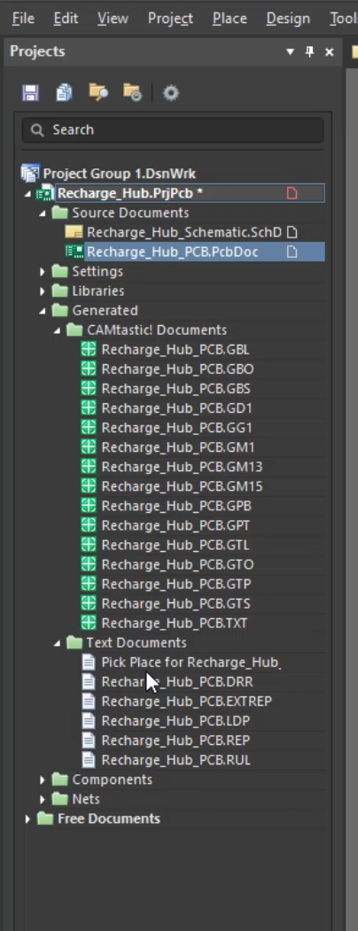
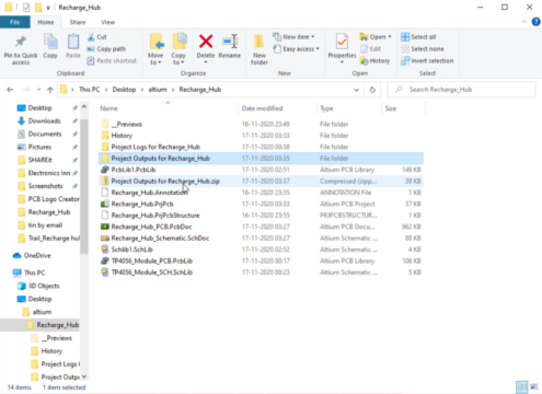
as you can see here, The generated files are located under the project files, project outputs for recharge hub directory, we need to send these files to PCBway.com, to get our PCBs manufactured. So, let’s generate a zip file of these files to transfer easily. So, the Zip file is created successfully. Finally, the PCB designing and generation of the fabrication files process is completed. we will order PCBs on PCBay.com using these files in the next episode.
Summary:
Coming to the summary of the episode, First of all, we have created this schematic document and added this Battery holder with the help of this Altium library loader, Then we have created own schematic and PCB library for the TP4056 module and added to the schematic then added few more components, and connected all the components. Then transferred all these files to the PCB File and fine-tuned the PCB placement and completed the PCB routing part. Then added a few branding strings and logos, and Then generated PCB fabrication files,
thus completed the final PCB Designing part.
So, that’s it for this tutorial. see you in the next episode bye…bye…